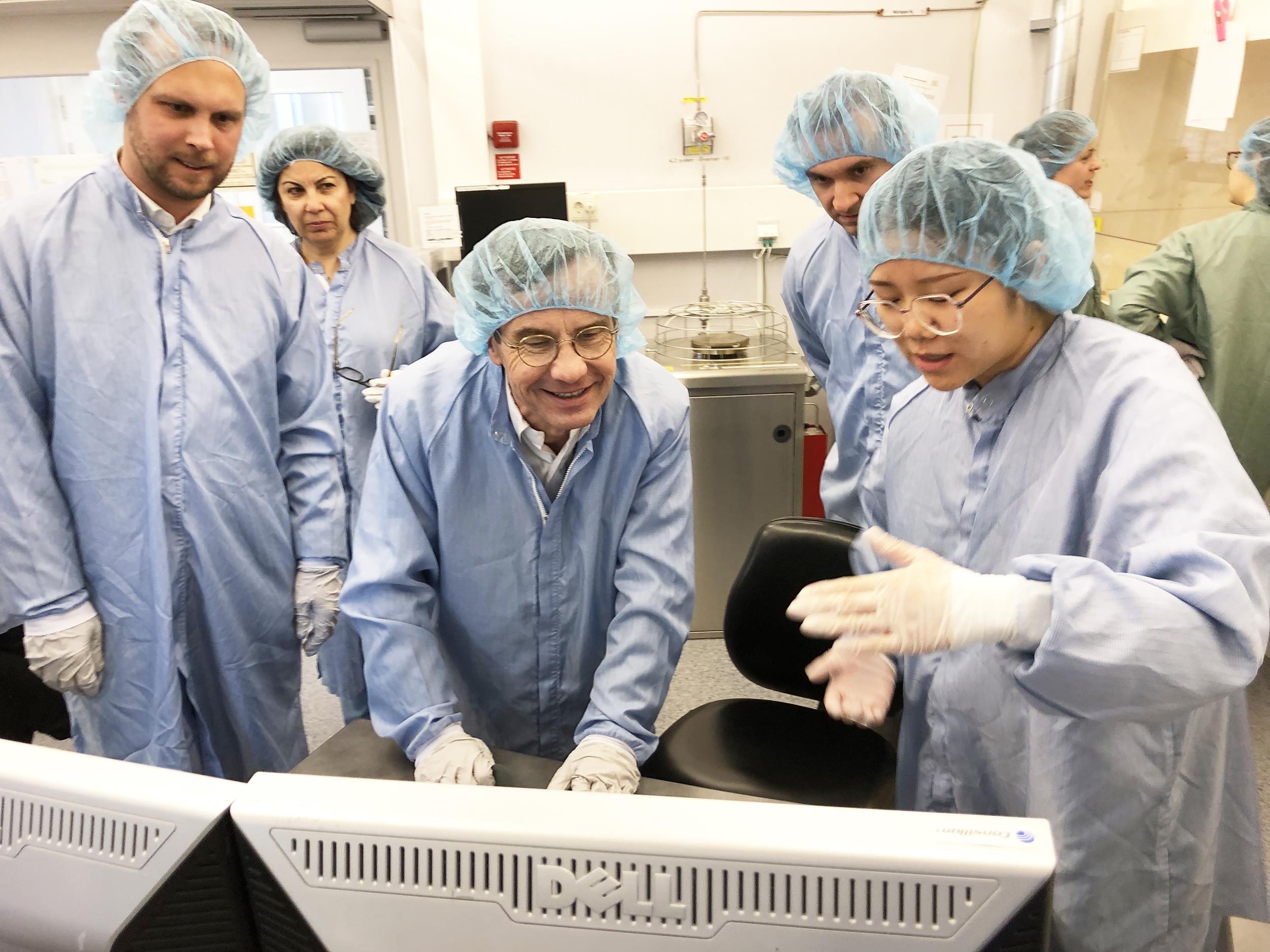
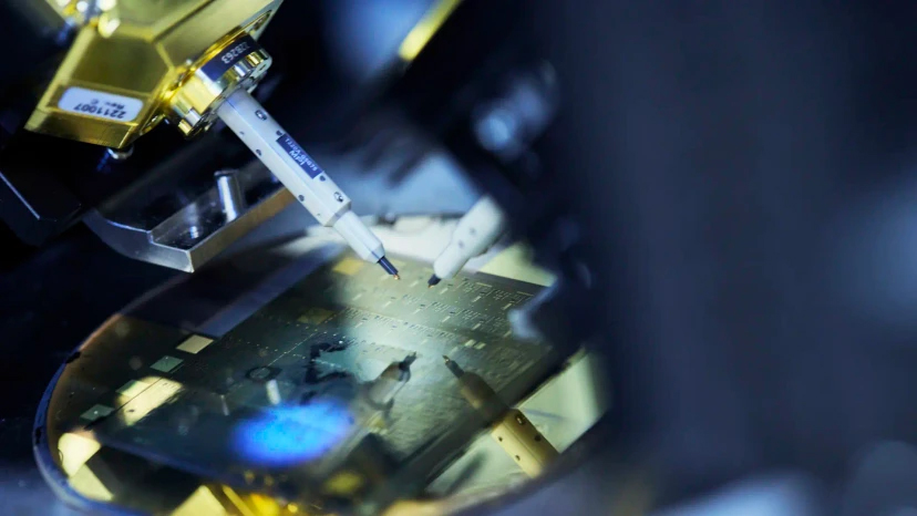
Semiconductors – the “brains” behind electronic products and systems. Whether mobile phones, automotive, energy, home appliances, or artificial intelligence, these components (“chips”) play a key role. At the same time, Asian countries account for more than half of the world’s semiconductor chip production. Swedish semiconductor capability is now to be strengthened by Lund University together with Chalmers and KTH.
“Our three universities strive to work together to strengthen the competitiveness of Swedish industry and society for digitalisation, security, and the green transition. In a troubled world, we create independence and contribute to ensuring Europe access to critical components,” says Erik Renström, Vice-Chancellor of Lund University.
|
|
|
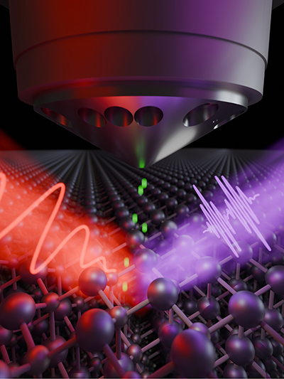
In a study, Jan Vogelsang, Lukas Wittenbecher, Sara Mikaelsson, Chen Guo, Ivan Sytcevich, Anne-Lise Viotti, Cord L. Arnold, Anne L’Huillier, and Anders Mikkelsen demonstrate a clear pathway for attosecond interferometry with high spatial resolution at atomic scale surface regions.
A pair of extreme ultraviolet attosecond pulses photoemits electrons from the surface of a zinc oxide crystal, while experiencing the field of a time-delayed, near-infrared (NIR) probe pulse. The photoelectrons are recorded with a photoemission electron microscope (PEEM), resulting in spatially resolved attosecond interferometry. This is the first time photoelectron cross-correlation traces were recorded with a PEEM as a detector. It is a step towards attosecond time-resolved and nanometer spatially resolved photoelectron emission time measurements.
|
|
|
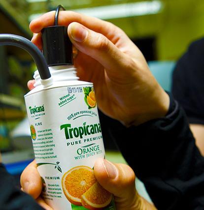
“You need to build deep knowledge and do academic research in parallel with industrial development. Programs like WISE provide this opportunity,” says Tetra Pak’s Eva Gustavsson.
Tetra Pak and Lund University join forces in a shared research project as part of WISE (The Wallenberg Initiative Materials Science for Sustainability). In this project, the target is the research and development of packaging materials that are fully recyclable and that contribute to reducing the CO2 footprint.
|
|
|
Roughly 80 percent of all chemical products are manufactured using catalysts. The Swedish Foundation for Strategic Research (SSF) has made a movie with one of their Future Research Leaders, our deputy director, professor Maria Messing. Her research group uses spark discharge generation to obtain more efficient and environmentally friendly processes in manufacturing nano-sized catalysts.
|
|
|
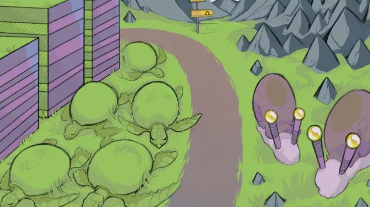
Anastasia Tsioki is in her first year of the engineering programme in technical nanoscience at LTH. In high school, she took a science programme focusing on design. Jonas Johansson is the programme manager and teacher, a professor of physics and develops new knowledge for producing materials at the nanoscale. When Jonas was about to publish a scientific article, he turned to Anastasia to illustrate a proposed cover image. The magazine immediately accepted her illustration as the front-page image.
“Basically, a diagram of turtles and snails”
|
|
|
In mid-February, thousands of European early-stage researchers received their applications for EU Marie Curie Postdoctoral Fellowship funding. The question is: how do you succeed with your Marie Curie application? Konstantin Nestmann, a postdoc at NanoLund, scored 100 out of 100 points. The magazine Curie, published by the Swedish Research Council, talked with him about this.
|
|
|
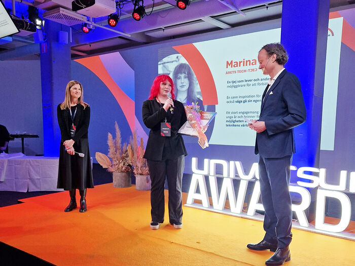
Our warmest gratulations to Marina Peltonen, who is studying for an MSc in Engineering Nanoscience at LTH! This award has been presented for over two decades to inspire more girls and young women to choose an education or career in tech.
“I feel incredibly honoured to receive this award and see this as an amazing opportunity to work with Microsoft on important social issues. It’s great that they chose me, who has an interdisciplinary background. I see it as an important mission to inspire more girls to apply for technical programmes and thus increase gender equality in the industry,” says Marina Peltonen.
The motivation for her award is: “A girl who lives and breathes tech as an enabler to improve our society. A true inspiration for young women – to dare and to have the courage to go their own way. A great commitment to the world of research from a young age and passionate about giving all students in school the opportunity to test and be inspired by the world of technology.”
|
|
|
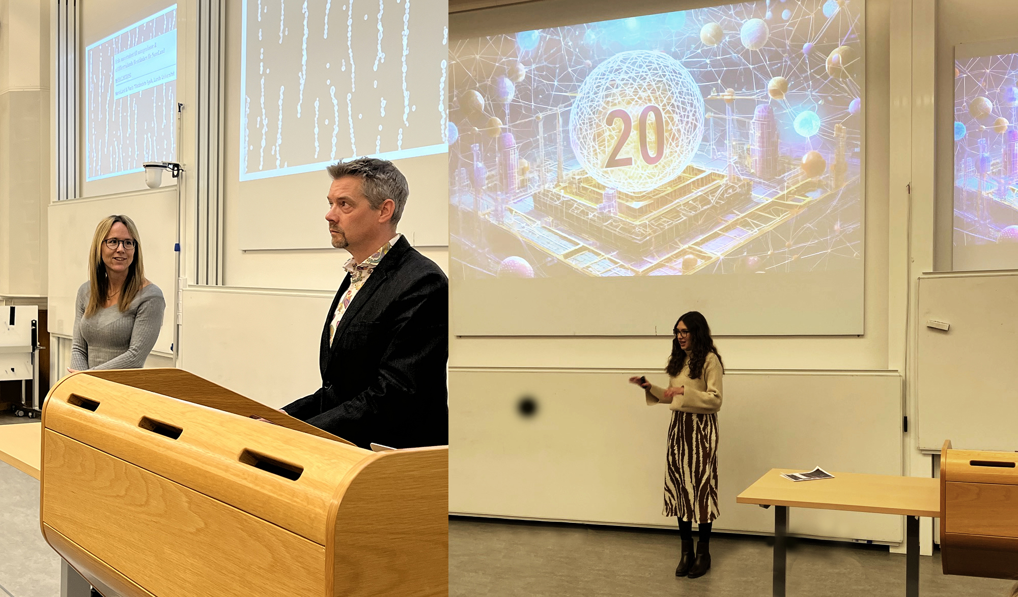
For twenty years now, LTH has educated students in the programme Master of Science in Engineering Nanoscience. Jonas Johansson has led the programme since 2020 and he states:
“Some parts of the programme are the same as when it started twenty years ago – but it has evolved a lot, and continues to do so. For example, we have recently introduced optional courses in AI and this autumn we will launch a new specialisation in energy systems. Engineering nanoscience is a programme that is unique in Sweden. It is the only MSc programme with nanoscience as a consistent theme throughout all five years. Our students help to blur the boundaries between traditional areas of knowledge such as biology, physics, chemistry, materials science and electronics. They become MSc engineers with cutting-edge skills, gained through their specialisation, and interdisciplinary expertise.”
|
|
|
Compound Semiconductor Week (CSW) is the premier conference in the field of science, technology, and applications of compound semiconductors, and it will be arranged in Lund on 3–6 June 2024.
CSW addresses compound semiconductors from fundamentals to applications in a wide perspective. CSW covers new developments in materials and physics while simultaneously addressing applications in electronics, optoelectronics, and new fields. With its annual coverage, CSW is a forum for the latest developments in this important field.
The conference covers the following areas:- Materials Epitaxy, Fabrication and Characterization
- Device Technology and Applications
- Nano and quantum Physics
|
|
|
Nano for computing and computing for nano – the theme of the annual meeting will be computing and nano in a broad sense. This will include using new computational methods such as machine learning and artificial intelligence to benefit nanoscience research, as well as using nanoscience to create new computational paradigms, including biological-, neuromorphic- and quantum computing.
|
|
|
Did you know that there are several support and funding opportunities for NanoLundians? NanoLund offers our members support in high-impact publishing.
As a member, you can get hands-on help from experienced editors to achieve the highest impact and visibility of your work. If you have an important result that you think should be published in one of the top journals in your field, contact Anna-Karin Alm.
|
|
|
Welcome to an information meeting about Lund Nano Lab (LNL) – what is it, what does it offer and how can you access it? We will also tell you about the plans and process of building the new Nano Lab at Science Village, a cutting-edge semiconductor nanofabrication facility near MAX IV and ESS.
We will offer a tour of the lab for those interested – places for the tour are limited and pre-registration is compulsory. More information about registration for the lab tour is found in the registration form for the information meeting (see link below).
|
|
|
|